As electronic devices grow more complex, chip-level repair is essential to maintain performance and extend lifespan. BGA chip soldering quality directly impacts device reliability. In this article, Phonefix introduces solder ball stencils for electronic chips, helping technicians quickly grasp key usage tips to enhance repair efficiency and quality.

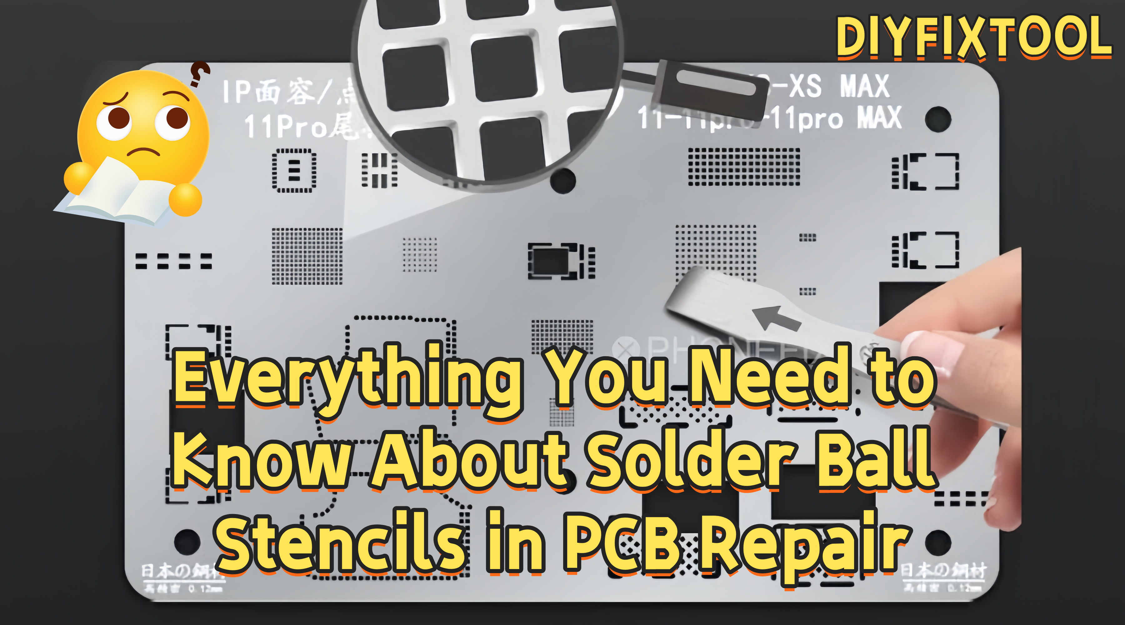
I. Solder Ball Stencils Overview
Solder ball stencils are critical tools used to accurately place solder balls onto chip pads, ensuring soldering quality and efficiency.
1. Introduction
· Made of durable stainless steel, typically 0.08–0.15mm thick.
· Common types: single-layer, framed , and high-accuracy laser-cut stencils.
· Apertures are slightly larger than Solder Balls ; pitch must match pad layout.
2. Main Functions
· Accurately positions solder balls on chip pads, essential for rework and reballing.
· Maintains consistent ball size and placement to improve soldering quality and electrical performance.
· Reusable to reduce repair waste and avoid damage to chips and pads.

II. Soldering Methods
Currently, there are two main solder application methods for BGA chip repair. The choice depends on actual repair needs:
1. Solder paste application
Applying solder paste through the stencil onto pads; suitable for repairs requiring simple operation and high flexibility. Stencil design considers aperture size and thickness to ensure uniform solder paste formation, convenient for individual repairers.
2. Solder ball placement
Preformed solder balls are placed into stencil holes and then melted by heating with a BGA Soldering Station. This process requires high precision in stencil aperture size and material.

III. Stencil Selection and Aperture Matching
1. Stencil selection:Select appropriate stencil based on the chip's package and pad layout. Obtain the chip model and package parameters in advance.
2. Model search:Use third-party platforms to search stencil models by chip model or prefix keywords, or compare stencil classification images to choose similar models.
3. Aperture tolerance:Aperture size is generally designed according to pad size. When using Solder Paste, exact aperture size is less critical if the paste is applied evenly.
4. Ball size matching:For solder ball placement, use solder balls matching the chip’s original ball diameter. Small batch testing is recommended for first-time use.

IV. Solder Ball Placement Process Steps
Step 1:Choose a stencil that matches the chip pad size and shape, ensuring the aperture fits the solder balls. A Magnetic Silicone Mat is placed underneath to protect the surface and keep components organized. Stencils can be selected by either searching the chip model or comparing pad structures.
Step 2: Apply solder paste evenly or place appropriately sized solder balls into stencil holes, ensuring full coverage. Ball size should match the chip’s original spec, with small-batch testing for first-time use. Use mid-temp paste (~183°C) for general repairs, high-temp lead-free (~217°C) for high-heat or eco-sensitive cases, and low-temp (~138°C) for heat-sensitive components.

Step 3: Precisely align the stencil with chip pads, then uniformly heat with YCS Hot Air Gun to melt solder paste or solder balls, bonding them to pads. Control temperature carefully to avoid stencil deformation or chip damage; maintain proper hot air gun distance and ensure even heating.
Step 4: After solder material cools and solidifies, carefully remove stencil to avoid solder strings and chip displacement, completing the solder ball placement process. Beginners are advised to practice on small package chips first, using a bumping soldering platform to improve paste application stability and avoid insufficient or excessive solder.

V. FAQ
The following addresses common issues encountered during use of electronic chip stencils and their solutions:
1. How to solder when capacitors and resistors are on the chip?
Most stencils partially mask capacitor and resistor areas, preventing solder paste from covering these components. If components protrude significantly, scrape solder paste carefully to avoid overflow.
2. Can a single stencil be used for solder ball placement?
For small package chips, a single stencil can be used along with hot air gun heating. For larger chips, a Middle Layer Reballing Stencil is recommended in combination with a bumping solder platform to ensure proper alignment and solder joint quality.
3. What stencil options exist for EMMC chips?
EMMC commonly uses BGA153 and BGA169 packages; general models such as EMMC3 fit most cases and should be preferred for repairs.

VI. Conclusion
Correct selection and operation of solder ball stencils for electronic chips are key to ensuring repair quality. Understanding soldering methods, reasonably choosing stencil models and solder paste, and mastering heating techniques can greatly improve solder joint yield and repair efficiency. For more information on solder ball placement or professional tools, please visit the DIYFIXTOOL official website.