
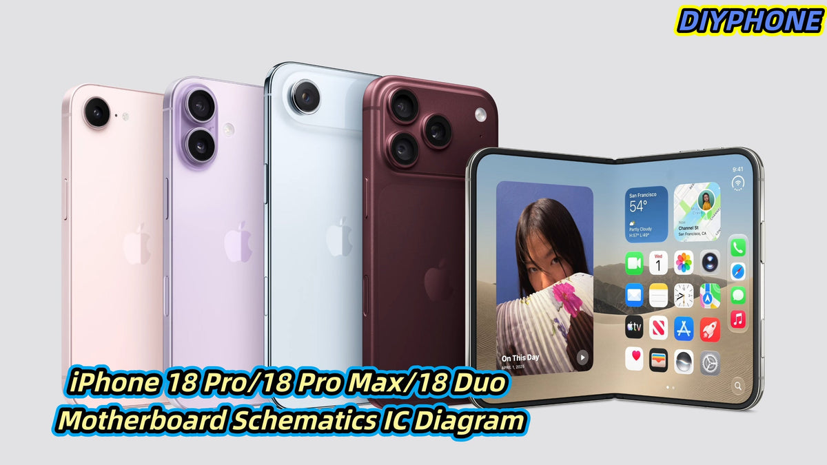
As the new generation of iPhones attracts attention, the motherboard designs and IC component layouts of the iPhone 18 Pro, iPhone 18 Pro Max, and iPhone 18 Duo have also become hot topics of discussion in the mobile phone repair industry. Based on the currently available motherboard component layout diagrams, this article provides a reference for repair technicians. It is believed that online software tools such as JC Drawing, WUXINJI, ZXW, and XZZ Drawing will soon update their iPhone 18 motherboard circuit diagrams and bitmap layouts.

Overview of the iPhone 18 Series Design
The iPhone 18 series is expected to continue covering different product form factors, including high-end conventional smartphones and foldable-screen devices. The iPhone 18 Pro and iPhone 18 Pro Max will focus on performance, imaging, display quality, and battery life, while the iPhone 18 Duo will feature a foldable-screen design as its main highlight. Different models may vary in screen form factor, body structure, camera configuration, and internal space layout to meet the needs of different users.
For the iPhone 18 Pro and iPhone 18 Pro Max, key areas of user interest include the next-generation processor, camera system, display technology, wireless connectivity, and battery life. The foldable-screen concept model, iPhone 18 Duo, needs to balance the large-screen experience when unfolded, portability when folded, and coordinated design among the hinge, flexible display, and body structure.
iPhone 18 Pro/18 Pro Max Motherboard (RF Board IC Components)
According to the currently available diagrams, the relevant motherboard areas of the iPhone 18 Pro and iPhone 18 Pro Max involve circuits for the charging port, battery connector, baseband, RF, NFC, Wi-Fi/Bluetooth, and camera power supply. The main components include the charging IC, battery connector, baseband and baseband power supply, RF transceiver circuits (RF/WTR), power amplifiers (PA), NFC circuits, and other FPC connectors.
The baseband is responsible for digital signal processing in cellular communications, while the RF transceiver circuits handle the transmission and reception of wireless signals. The power amplifier is used to amplify transmitted signals. The NFC circuit supports near-field communication, while the Wi-Fi/Bluetooth module is used for wireless networking and peripheral connections. The charging IC and battery connector handle charging and power transmission, while other FPC connectors are used to connect the display, cameras, or other peripheral components.
These functional areas collectively form the phone's communication and interface systems. When dealing with no service, abnormal signal reception, or charging failures, the relevant power supplies, connectors, and signal paths should be examined together, rather than diagnosing faults based solely on component locations.

iPhone 18 Pro/18 Pro Max Motherboard (AP Board IC Distribution)
The AP board primarily revolves around the application processor and its peripheral circuits, involving functional modules such as the processor, power management, wireless connectivity, display, camera, and audio. The main components labeled in the diagram include:
· A20 Pro CPU: Responsible for system computing, application execution, and related control tasks.
· PMU/PMIC: Provides the required voltages for different circuits and coordinates the power supply status of each module.
· Wireless charging-related circuits: Responsible for receiving wireless charging energy and related control functions.
· Wi-Fi/Bluetooth module: Supports wireless networking and Bluetooth device connections.
· Camera power supply IC: Provides power to camera modules and related circuits.
· Display IC: Involves display driving or related control functions.
· Flash IC: Controls the power supply and operating status of the LED flash.
· Audio and sensor-related circuits: Involve sound capture, processing, and output, as well as motion sensing and orientation detection.
These components collectively form the main functional areas of the AP board, with each module working in coordination through power supply lines and signal paths. Repair technicians can focus on inspecting the relevant power supplies, connectors, and peripheral circuits based on the observed fault symptoms.

iPhone 18 Duo Foldable-Screen Motherboard Component Layout Diagram
Based on the currently available iPhone 18 Fold foldable-screen diagram, the motherboard adopts a layout consisting of multiple circuit board areas, including a main logic board and a long, narrow auxiliary circuit board. The main components shown include the processor, power management IC, baseband and RF circuits, Wi-Fi/Bluetooth module, NFC, wireless charging-related circuits, camera power supply IC, display IC, audio circuits, and various connectors.
The motherboard design of a foldable-screen device needs to accommodate the space on both sides of the body, the hinge structure, connections to the inner and outer displays, and heat dissipation requirements. Compared with traditional conventional smartphones, the layout of flexible cables and connectors deserves greater attention.
iPhone 18 Pro/18 Pro Max/18 Duo Motherboard Repair and Diagnostics
· During motherboard repairs, the inspection approach should be determined according to the fault symptoms, and the relevant circuits should be verified against the actual model and motherboard version.
· Power supply faults: Check the battery input, power management outputs, and relevant power rails to identify short circuits, missing power supplies, or abnormal voltage drops.
· Communication faults: Check the baseband, RF front end, antenna connections, and related power supplies to analyze issues such as no service, weak signals, or unstable connectivity.

· Charging faults: Check the charging port, battery connector, charging management circuit, and related power paths.
Display faults: Check the display connector, flexible cable, related power supplies, and signal paths.
Camera and audio faults: Check peripheral modules, connectors, and related control circuits, gradually narrowing down the scope of inspection based on the fault symptoms.
Repair technicians should prioritize using schematics, bitmap layouts, and measurement data that match the target motherboard, avoiding judgments about chip models or direct component replacement based solely on schematic diagrams.
The above is a preliminary analysis of the motherboard component layouts of the iPhone 18 Pro, iPhone 18 Pro Max, and iPhone 18 Duo, covering major functional areas such as the processor, power management, communications, display, camera, and audio. The relevant chip models and specific layouts still need further verification. Going forward, PHONEFIX will continue to supplement this information based on reliable physical teardowns, schematics, and repair documentation to provide references for mobile phone repair technicians.


