
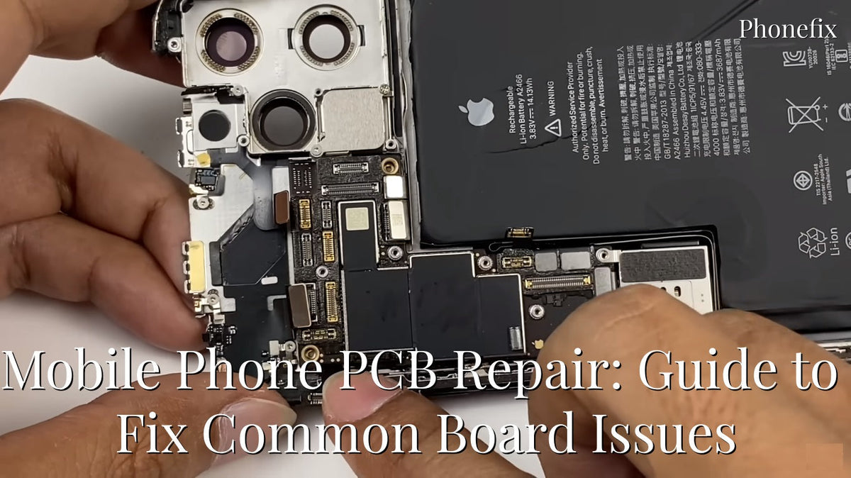
Board-level repair saves devices that screen swaps and battery replacements cannot fix. It demands patience, correct tools, and a methodical diagnostic process. This guide explains what phone PCB repair involves, the tools needed, the step-by-step repair process, why proper technique matters, and common beginner mistakes.

I. What Board-Level Phone Repair Actually Involves
· PCB repair means fixing faults on the phone's main circuit board. The board is also called the logic board or motherboard.
· Repair happens at board level. The whole board is not replaced.
· A modern phone board stacks ten or more layers of copper traces. Some traces are thinner than a human hair.
· Hundreds of tiny parts sit on these layers: resistors, capacitors, ICs, and connectors.
· One failed charging IC or one cracked trace can make the phone look dead. The rest of the board may still work perfectly.
· The industry standard is IPC-7711/7721. It defines acceptable procedures for component rework and board repair.
· Rework restores a board to its original condition.
· Repair makes the board electrically functional after physical alteration. A jumper wire bridging a broken trace is one example.
II. Tools You Need Before Starting
· Digital multimeter: for continuity and voltage testing.
· Temperature-controlled soldering iron: tip temperature 300–380°C.
· Hot air rework station: adjustable temperature and airflow.
· Fine-point tweezers.
· Desoldering braid.
· 90%+ isopropyl alcohol.
· No-clean flux.
· Magnification: 10–40x.
· ESD wrist strap and anti-static mat.
ESD protection is not optional. Electrostatic discharge can damage ICs invisibly. The failure may not show up for weeks.
III. Step-by-Step PCB Repair Process for Beginners
Step 1: Visual Inspection Under Magnification
· Place the board under a 10x loupe or stereo microscope.
· Photograph the board from multiple angles.
· Document component positions.
Look for:
· Burnt components: darkened epoxy or cracked ceramic bodies.
· Cold solder joints: dull or grainy appearance.
· Cracked or lifted traces.
· Corrosion: green or white deposits on copper.
This step costs nothing. It often reveals the fault immediately.
Step 2: Basic Continuity and Short Testing
· Keep the board unpowered.
· Set the multimeter to diode mode or continuity mode.
· Connect the red probe to ground.
· Touch the black probe to test points.
· Check the battery connector first.
Readings:
· Healthy phone board: 0.200V to 0.700V in diode mode.
· Near zero: short.
· OL (open loop): broken connection.
Test power rails for shorts. Measure VCC to ground. If a rail reads short, every component on that line may also read short. Visual clues become important. They help locate the real culprit.
Step 3: Isolating the Faulty Section
· Narrow the fault to a specific circuit.
· Use schematics or boardview files.
· Trace signal paths.
· Compare expected values with multimeter readings.
Examples:
· Phone does not charge: check the charging IC and nearby components.
· Phone boots but screen shows nothing: check the backlight circuit.
This step separates professional repair from guesswork. Repair community notes a simple rule. Use visual clues and logical deduction. The part that does not work tells where to look first.
Step 4: Component-Level Diagnosis
· Test individual components in-circuit where possible.
· Check resistors and diodes without desoldering when possible.
· For ICs, check power pins for shorts.
· Look for abnormal diode readings.
· Use a thermal camera. A failed component often runs hotter than its neighbors.
· Inject controlled voltage into a shorted rail. Use freeze spray to find the component that melts first.
Be patient. Rushed diagnosis leads to unnecessary part removal. It also risks damaging the board.

Step 5: Safe SMD Removal with Proper Heat
Small components (resistors, capacitors):
· Use a vertical-wind hot air gun.
· Set temperature to 330–365°C.
· Set airflow around 1–3.
· Hold the nozzle 3–6 mm from the component.
· Heat evenly for 13–18 seconds.
· Lift with tweezers.
Larger chips (NAND, power management ICs):
· Use a helical-wind gun.
· Set temperature to 365–400°C.
· Set airflow around 45–65.
Safety:
· Apply high-temperature tape around the component.
· Protect nearby parts.
· Keep the nozzle vertical.
· Never rush removal. Uneven heating cracks nearby components.
Step 6: Trace Repair and Jumper Wiring
· Use 0.1mm enamelled copper wire for phone board work.
· Clean the exposed trace with flux and isopropyl alcohol.
· Tin the trace with a thin layer of solder.
· Cut a jumper wire slightly longer than needed.
· Solder one end to the damaged trace.
· Route it to the next connection point past the break.
For lifted pads:
· Reconstruct the pad with adhesive-backed copper foil.
· Solder the component back in place.
· Apply UV-curable solder mask over the repaired area.
Keep jumper wires short and direct. This minimizes signal interference.
Step 7: Cleaning and Final Testing
· Clean the repaired area with 90%+ isopropyl alcohol and a soft brush.
· Remove flux residue. Leftover flux attracts moisture and causes corrosion.
· Perform a full continuity check on all repaired connections.
· Power the board through a DC power supply.
· Set current limiting low. This prevents further damage if a short remains.
If the board boots:
· Test charging.
· Test display and touch.
· Test audio and cameras.
· Test wireless connectivity.
A repair that passes these tests is ready to go back into the phone.
IV. Why Proper Technique Matters
· 2025 IPC repair workshop data: roughly 62–68% of "dead" boards sent for replacement could be repaired safely. Methodical troubleshooting makes the difference.
· The same data shows rushed repairs cause most repeat failures within 90 days.
· Proper technique preserves device data. On modern phones, the storage chip sits directly on the board. Replacing the whole board means losing everything.
· The EU's Right to Repair Directive took effect for smartphones on June 20, 2025.
· It requires manufacturers to provide spare parts and repair information for at least seven years after the last unit is sold.
· Board-level repair skills align directly with this regulatory shift.
V. Common Beginner Mistakes
1. Applying too much heat.
· Excessive temperature lifts nearby pads.
· It damages the laminate underneath.
· Start at the lower end of the temperature range.
· Increase only if needed.
2. Skipping flux.
· Flux helps solder flow smoothly.
· It prevents oxidation.
· Soldering without flux creates cold, unreliable joints.
3. Forgetting ESD protection.
· A small static discharge from fingers can kill a charging IC.
· There may be no visible sign.
· Wear a grounded wrist strap.
· Work on an anti-static mat.
· This costs almost nothing and prevents invisible damage.
4. Repairing without a confirmed diagnosis.
· Desoldering components at random wastes time.
· It introduces new faults.
· Follow the diagnostic sequence: visual inspection, continuity testing, voltage mapping.
· Pick up the soldering iron only after that.

Board-level repair is a skill built through practice. Start with dead boards from old phones. Work through the diagnostic steps until they become second nature. A good set of Phone Repair Tools makes the learning process safer and more productive. The techniques in this guide form the foundation; experience fills in the rest.


